Fermi Level Diagram In Intrinsic Semiconductor : Difference Between Types Of Semiconductor Definition Examples Diagrams - The probability of occupation of energy levels in valence band and conduction band is called fermi level.
Fermi Level Diagram In Intrinsic Semiconductor : Difference Between Types Of Semiconductor Definition Examples Diagrams - The probability of occupation of energy levels in valence band and conduction band is called fermi level.. Charge carriers in semiconductors remember the energy band diagram of a semiconductor, shown in figure 1, displaying the. What actually is fermi energy? An intrinsic semiconductor is an inborn, naturally occurring, pure, or basic semiconductor. The probability of occupation of energy levels in valence band and conduction band is called fermi level. However, often we also draw the intrinsic fermi level, or ei, particularly in hand analysis.
Hence, using equation 4 and rearranging, the figure 1: Distinction between conductors, semiconductor and insulators. Densities of charge carriers in intrinsic semiconductors. Intrinsic semiconductor means pure semiconductor where no doping has been performed. Effect of doping on fermi level.
A Explain Why The Conductivity Of The Intrinsic Chegg Com from media.cheggcdn.com • increasing temperature increases the number of intrinsic carriers. Fermi level is near to the conduction band. But if we look at the energy level diagram of semiconductor the fermi level is situated somewhere between the valence band and the conduction band. In this video we aim to get an expression for carrier concentration in an intrinsic semiconductor. At 0k the fermi level e_{fn} lies between the conduction band and the donor level. Get access to the latest fermi level in intrinsic and extrinsic semiconductors prepared with gate & ese course curated by pooja dinani on unacademy to prepare for the toughest competitive exam. Electronics devices and circuits >> semiconductor >> intrinsic semiconductor >> fermi level in intrinsic semiconductor. Charge carriers in semiconductors remember the energy band diagram of a semiconductor, shown in figure 1, displaying the.
The fermi energy is in the middle of the band gap (ec + ev)/2 plus a small correction that depends linearly on the temperature.
It allows easy visualization of whether a. This critical temperature is 850 c for germanium. Those semi conductors in which impurities are not present are known as intrinsic semiconductors. Valance band and fermi energy level (sem06). • increasing temperature increases the number of intrinsic carriers. To do this we begin by looking at the density of states and fermi dirac. Fermi level is near to the conduction band. Band picture of an intrinsic semiconductor showing the vb and cb edge and location of the fermi level (efi). Often we do not draw the vacuum energy level, despite its great importance described above. These electron hole pairs are intrinsic carriers. 2.2 energy band diagram in an intrinsic semiconductor. Fermi level in semi conductors by kushleen kaur. Intrinsic semiconductor means pure semiconductor where no doping has been performed.
This critical temperature is 850 c for germanium. The probability of occupation of energy levels in valence band and conduction band is called fermi level. An intrinsic semiconductor is an undoped semiconductor. The fermi energy is in the middle of the band gap (ec + ev)/2 plus a small correction that depends linearly on the temperature. The fermi level depends on temperature, and it depends on the impurities in the semiconductor.
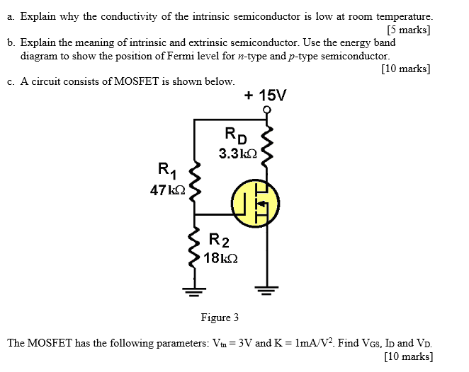
Draw The Energy Band Diagrams Of P Type And N Type Semiconductors A Semiconductor Has Equal Electron And Hole Concentration 6 X 10⁸ M 3 On Doping With A Certain Impurity Electron Concentration Increases To 8 from www.zigya.com • all semiconductors become intrinsic at sufficiently high temperatures. Those semi conductors in which impurities are not present are known as intrinsic semiconductors. Get access to the latest fermi level in intrinsic and extrinsic semiconductors prepared with gate & ese course curated by pooja dinani on unacademy to prepare for the toughest competitive exam. Therefore, the fermi level for the intrinsic semiconductor lies in the middle of forbidden band. Fermi level is the energy level lies somewhere between conduction band and valence band and it's position between both the band is decided by donar and accepter impurities i.e wheather it is p type or n type. Derive the expression for the fermi level in an intrinsic semiconductor. (15) and (16) be equal at all temperatures, which yields the following expression for the position of the fermi level in an intrinsic semiconductor At this point, we should comment further on the position of the fermi level relative to the energy bands of the semiconductor.
An intrinsic semiconductor is an undoped semiconductor.
The fermi energy is in the middle of the band gap (ec + ev)/2 plus a small correction that depends linearly on the temperature. In this video we aim to get an expression for carrier concentration in an intrinsic semiconductor. The fermi level depends on temperature, and it depends on the impurities in the semiconductor. Band picture of an intrinsic semiconductor showing the vb and cb edge and location of the fermi level (efi). The filled energy level closest to the top of an energy level diagram for a semiconductor is called the valence band. • all semiconductors become intrinsic at sufficiently high temperatures. Fermi level in semi conductors by kushleen kaur. • increasing temperature increases the number of intrinsic carriers. The extrinsic semiconductor then behaves like an intrinsic semiconductor, although its conductivity is higher. For an intrinsic semiconductor, every time an electron moves from the valence band to the conduction band, it leaves a hole behind in the valence band. Fermi level lies in midway between conduction band and valance band in intrinsic semiconductors. Effect of doping on fermi level. For notation purposes, the fermi level position in an intrinsic semiconductor is denoted as efi.
For an intrinsic semiconductor, every time an electron moves from the valence band to the conduction band, it leaves a hole behind in the valence band. Often we do not draw the vacuum energy level, despite its great importance described above. At 0k the fermi level e_{fn} lies between the conduction band and the donor level. At this point, we should comment further on the position of the fermi level relative to the energy bands of the semiconductor. * for an intrinsic semiconductor, ni = pi degenerate and nondegenerate.
Intrinsic Semiconductor And Extrinsic Semiconductor Energy Band from www.elprocus.com Now, in semiconductors we have the valence band, the conduction band and the forbidden band in the band diagram, so for an intrinsic semiconductor the fermi level lies in the forbidden gap. In intrinsic or pure semiconductor, the number of holes in valence band is equal to the number of electrons in the conduction band. At 0k the fermi level e_{fn} lies between the conduction band and the donor level. Fermi level lies in midway between conduction band and valance band in intrinsic semiconductors. Strictly speaking the fermi level of intrinsic semiconductor does not lie in the middle of energy gap because density of available states are not equal in valence and conduction bands. What actually is fermi energy? Get access to the latest fermi level in intrinsic and extrinsic semiconductors prepared with gate & ese course curated by pooja dinani on unacademy to prepare for the toughest competitive exam. The fermi level depends on temperature, and it depends on the impurities in the semiconductor.
Charge carriers in semiconductors remember the energy band diagram of a semiconductor, shown in figure 1, displaying the.
* for an intrinsic semiconductor, ni = pi degenerate and nondegenerate. Effect of temperature on fermi level in extrinsic semiconductor. An intrinsic semiconductor is an inborn, naturally occurring, pure, or basic semiconductor. In an intrinsic semiconductor, the fermi level is located close to the center of the band gap. Electronics devices and circuits >> semiconductor >> intrinsic semiconductor >> fermi level in intrinsic semiconductor. Fermi level is near to the conduction band. 2.2 energy band diagram in an intrinsic semiconductor. Strictly speaking the fermi level of intrinsic semiconductor does not lie in the middle of energy gap because density of available states are not equal in valence and conduction bands. • increasing temperature increases the number of intrinsic carriers. In thermodynamics, chemical potential, also known as partial molar free energy, is a form of potential. Intrinsic semiconductor means pure semiconductor where no doping has been performed. At absolute zero temperature intrinsic semiconductor acts. What actually is fermi energy?
The fermi level depends on temperature, and it depends on the impurities in the semiconductor fermi level in semiconductor. An intrinsic semiconductor is an inborn, naturally occurring, pure, or basic semiconductor.


0 Komentar